- 您现在的位置:买卖IC网 > Sheet目录312 > AT25F4096W-10SU-2.7 (Atmel)IC FLASH 4MBIT 33MHZ 8SOIC
�� �
�
�Features�
�?� Serial� Peripheral� Interface� (SPI)� Compatible�
�?� Supports� SPI� Modes� 0� (0,0)� and� 3� (1,1)�
�–� Datasheet� describes� Mode� 0� Operation�
�?� 33� MHz� Clock� Rate�
�?� Byte� Mode� and� 256-byte� Page� Mode� for� Program� Operations�
�?� Sector� Architecture:�
�–� Eight� Sectors� with� 64K� Bytes� Each� (4M)�
�–� 256� Pages� per� Sector�
�?�
�?�
�?�
�?�
�?�
�?�
�?�
�?�
�?�
�Product� Identification� Mode�
�Low-voltage� Operation�
�–� 2.7� (V� CC� =� 2.7V� to� 3.6V)�
�Sector� Write� Protection�
�–� Protect� 1/8,� 1/4,� 1/2� or� Entire� Array�
�Write� Protect� (WP)� Pin� and� Write� Disable� Instructions� for�
�both� Hardware� and� Software� Data� Protection�
�Self-timed� Program� Cycle� (30� μs/Byte� Typical)�
�Self-timed� Sector� Erase� Cycle� (1� second/Sector� Typical)�
�Single� Cycle� Reprogramming� (Erase� and� Program)� for� Status� Register�
�High� Reliability�
�–� Endurance:� 10,000� Write� Cycles� Typical�
�–� Data� Retention:� 20� Years�
�8-lead� EIAJ� SOIC� and� 8-lead� Small� Array� Package� (SAP)�
�4Mbit� High�
�Speed� SPI�
�Serial� Flash�
�Memory�
�4M� (524,288� x� 8)�
�AT25F4096�
�Description�
�The� AT25F4096� provides� 4,194,304� bits� of� serial� reprogrammable� Flash� memory�
�organized� as� 524,288� words� of� 8� bits� each.� The� device� is� optimized� for� use� in� many�
�industrial� and� commercial� applications� where� low-power� and� low-voltage� operation�
�are� essential.� The� AT25F4096� is� available� in� a� space-saving� 8-lead� EIAJ� SOIC� and� 8-�
�lead� SAP� packages.�
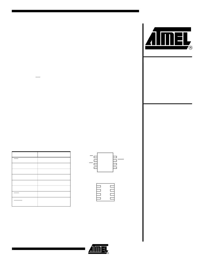
�Table� 1.� Pin� Configurations�
�8-lead� EIAJ� SOIC�
�Pin� Name�
�CS�
�SCK�
�Function�
�Chip� Select�
�Serial� Data� Clock�
�CS�
�SO�
�WP�
�GND�
�1�
�2�
�3�
�4�
�8�
�7�
�6�
�5�
�VCC�
�HOLD�
�SCK�
�SI�
�SI�
�Serial� Data� Input�
�SO�
�GND�
�Serial� Data� Output�
�Ground�
�8-lead� SAP�
�___�
�_____� 8�
�___�
�VCC�
�WP�
�Power� Supply�
�Write� Protect�
�VCC�
�HOLD� 7�
�SCK� 6�
�1�
�2�
�3�
�CS�
�SO�
�WP�
�HOLD�
�Suspends� Serial�
�Input�
�SI� 5� 4�
�Bottom� View�
�GND�
�2454G–SFLSH–5/06�
�发布紧急采购,3分钟左右您将得到回复。
相关PDF资料
AT25HP512W2-10SI-2.7 SL383
IC EEPROM 512KBIT 10MHZ 16SOIC
AT26DF081A-SSU
IC FLASH 8MBIT 70MHZ 8SOIC
AT26DF161-SU
IC FLASH 16MBIT 66MHZ 8SOIC
AT26DF161A-MU
IC FLASH 16MBIT 70MHZ 8QFN
AT26DF321-SU
IC FLASH 32MBIT 66MHZ 8SOIC
AT27BV010-90JU
IC OTP 1MBIT 90NS 32PLCC
AT27BV020-90JU
IC OTP 2MBIT 90NS 32PLCC
AT27BV040-12JU
IC OTP 4MBIT 120NS 32PLCC
相关代理商/技术参数
AT25F4096Y4-10YH-2.7
制造商:ATMEL 制造商全称:ATMEL Corporation 功能描述:4Mbit High Speed SPI Serial Flash Memory
AT25F512
制造商:ATMEL 制造商全称:ATMEL Corporation 功能描述:SPI Serial Memory
AT25F512_04
制造商:ATMEL 制造商全称:ATMEL Corporation 功能描述:SPI Serial Memory
AT25F512A
制造商:ATMEL 制造商全称:ATMEL Corporation 功能描述:SPI EEPROM Product Qualification
AT25F512A_06
制造商:ATMEL 制造商全称:ATMEL Corporation 功能描述:512Kbit High Speed SPI Serial Flash Memory
AT25F512A-10TU-2.7 SL383
制造商:Atmel Corporation 功能描述:
AT25F512AN-10SH-2.7
功能描述:闪存 512K Bit High Speed SPI Serial 闪存 Mem
RoHS:否 制造商:ON Semiconductor 数据总线宽度:1 bit 存储类型:Flash 存储容量:2 MB 结构:256 K x 8 定时类型: 接口类型:SPI 访问时间: 电源电压-最大:3.6 V 电源电压-最小:2.3 V 最大工作电流:15 mA 工作温度:- 40 C to + 85 C 安装风格:SMD/SMT 封装 / 箱体: 封装:Reel
AT25F512AN-10SU-2.7
功能描述:闪存 FLASH 1M SPI 10K CYCLES- 10MS 2.7V RoHS:否 制造商:ON Semiconductor 数据总线宽度:1 bit 存储类型:Flash 存储容量:2 MB 结构:256 K x 8 定时类型: 接口类型:SPI 访问时间: 电源电压-最大:3.6 V 电源电压-最小:2.3 V 最大工作电流:15 mA 工作温度:- 40 C to + 85 C 安装风格:SMD/SMT 封装 / 箱体: 封装:Reel